Material characterization
Material characterization at the micro and nano level is performed at the FHV using a wide range of high-performance instruments. The portfolio here includes scanning electron microscopy (SEM), correlative Raman and atomic force microscopy, and µ-tomography.
Scanning Electron Microscopy (SEM)
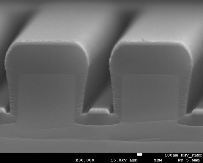
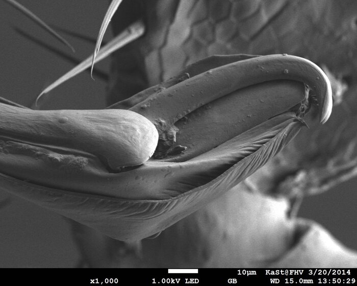
JEOL's JSM-7100F scanning electron microscope enables imaging and microscopic studies of both structure and chemical composition at the sample surface down to the nanometer scale. It offers very flexible measurement and characterization capabilities thanks to its wide range of detectors and measurement modes, and is suitable for a wide variety of different types of samples.
Some application examples:
-
Surface imaging of electrically conductive as well as poorly conductive or non-conductive samples.
-
Examination of non-conductive samples without prior metallization
-
Examination of biological samples.
-
Measurement of structures in the micrometer and nanometer range.
-
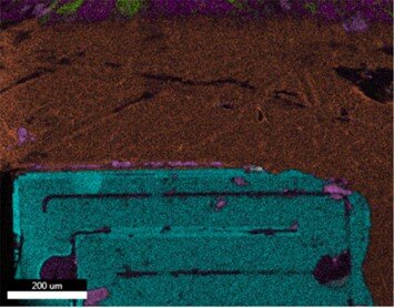
Qualitative and quantitative analysis of the chemical composition of the sample surface (elemental analysis, EDX) for the entire relevant range of the periodic table, also spatially resolved in the form of linescans or range mappings.
Specifications:
-
Magnification: 25 x to 1 000 000 x
-
Maximum resolution: 3.0 nm (depending on sample type, texture and size)
-
Maximum sample dimensions: 100 x 100 x 50 mm (L x W x H)
-
Elemental analysis (EDX):
-
Detection + quantification from boron (Z = 5) to bismuth (Z = 83)
-
Detection limit: approx. 0.5% by weight
Services:
-
REM imaging + structural dimension measurement
-
Analysis of chemical elemental composition of samples (qualitative + quantitative)
-
Elemental analysis and mappings of impurities, deposits, inclusions, etc.
-
Support in damage analysis, process failure investigations, and the like,
Contact
Raman correlative and atomic force microscopy (AFM)
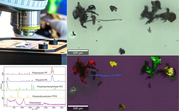
The WITec alpha300 RA enables correlative studies of chemical composition and surface topographies using Raman or atomic force microscopy.
Some application examples:
-
Chemical surface analysis of plastics, biomedical samples, food, semiconductors, dielectrics, or metallic compounds
-
Depth profile of chemical composition in transparent samples such as glasses or some plastics
-
Identification of the chemical fingerprint via the material database
-
Measuring the surface topography
Specifications:
Raman microscopy:
- Raman analysis of single points or mapping
- Measurement of surface profiles with AFM
- Consulting
Scanning force microscopy:
- Excitation wavelength: 405 nm, 532 nm, 785 nm
- Resolution: about 300 nm in x-y and about 900 nm in z
- Magnification: 10x, 20x, 50x, 100x
- Maximum sample size: approx. 100 x 100 x 20 mm
- Resolution approx. 1 nm
- Scan area 100 x 100 µm
- Contact and intermittent mode
Services:
-
Raman analysis of single points or mapping
-
Survey of surface profiles with AFM
-
Consulting
Contact
µ-tomography
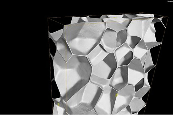
X-ray microinformatics is an imaging technique that enables the non-invasive and non-destructive characterization of the internal and external meso- and macrostructure of a sample in three dimensions with a spatial resolution on the order of one micrometer. Our instrument, GE's phoenix nanotom m, is ideally suited for metrology and microstructure characterization.
Some application examples:
-
Tube voltage range: 25-180 kV
-
Magnification x1.4 to x300
-
Detail detectability up to 0.2 µm
-
Minimum voxel size up to 0.3 µm
-
Maximum sample diameter: Ø240 mm
-
Maximum sample weight: 3 kg
Specifications:
-
Tube voltage range: 25-180 kV
-
Magnification x1.4 to x300
-
Detail detectability up to 0.2 µm
-
Minimum voxel size up to 0.3 µm
-
Maximum sample diameter: Ø240 mm
-
Maximum sample weight: 3 kg
Services:
-
Nondestructive and non-invasive imaging of components and materials
-
Characterization of material microstructure (e.g. porosity, filler content, connectivity analysis, n-point correlation functions, etc.)
-
Numerical simulation of multiphysics in domains based on tomography data
